The research interest of the thin-film nanomaterials area is very broad, covering aspects of of Solid State Chemistry and Physics. Our main research lines at this moment are:

4) Thin Film Nanomaterials:
1) Fabrication of oxide and nitride thin-films with improved thermoelectric efficiency.
Thermoelectric (TE) materials produce an electrical voltage in response to a temperature gradient. On a reverse version of this effect, thermoelectric cooling occurs when an electric current is passed through the system. Therefore, these materials can be used in thermoelectric energy conversion devices.
We are exploring the possibility of using low dimensional correlated oxides and nitrides (thin-films and multilayers) as TE materials. We try to exploit the effects of electronic and phononic confinement and interface scattering to optimize their thermoelectric performance.

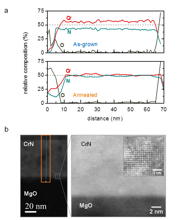
Figure: Microstructure of the interface between CrN and MgO with a high-resolution STEM image in the inset. Right: Dimensionless fi gure of merit of CrN films. ADVANCED MATERIALS, VOL 27, 3032, 2015.
2) Development of chemical methods of thin-film deposition (PAD – Polymer Assisted Deposition)
In the last few years, chemical solution deposition techniques emerged as a cheaper alternative to physical methods (MBE, PLD, sputtering, etc). Although the control of thickness, homogeneity and stoichiometry is still not competitive with physical techniques, the quality of the films is improving very fast. We use polymer assisted deposition (PAD) for the fabrication of thin-films of many materials with different properties, starting from environmentally friendly water solutions of biocompatible polymers.
Using this method, we were able to synthesize high quality films and multilayers of different oxides, with different properties, and over very large areas.

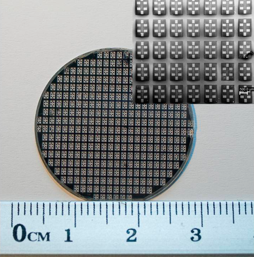
Figure 1: Left: High-resolution STEM image and EELS analysis of a 15 nm film of YIG prepared by Polymer Assisted Depositon (PAD) on GdGa Garnet. PHYSICAL REVIEW MATERIALS 1, 074407, 2017. Right: Epitaxial thin film of LaMnO3, 20 nm thick, deposited in a substrate of 1″-STO (chemical deposition). Optical photolithography was used to define 340 Hall bars (see inset). Results demonstrate an exceptional electrical homogeneity over the whole area. ACS APPLIED MATERIALS AND INTERFACES VOL 7, 5410, 2015
PHYSICAL REVIEW LETTERS, 115, 166801, 2015. PHYSICAL REVIEW B 95, 165138, 2017. SMALL 13, 1701614, 2017
3) We are also working on the ERC – Proof a Concept “ANTS”: A new technology of microthermal sensing for application in microcalorimetry (2017-2018), based on patented results obtained within the ERC – StG “2DTHERMS” (2010-2015)
This project aims to prove the viability of a novel thermal microsensor to develop a High-Throughput Calorimetry going beyond the current capabilities on Isothermal Titration Calorimetry (ITC).

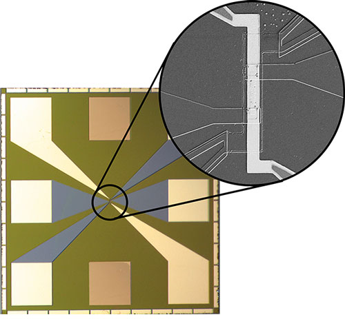
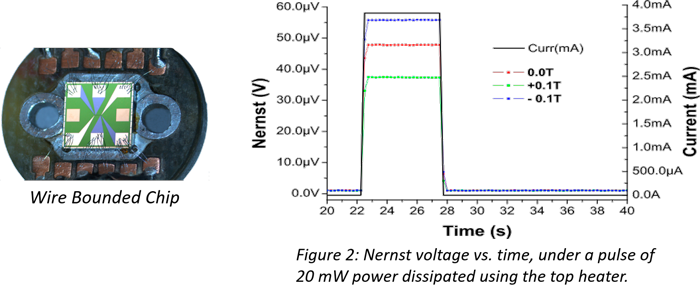
Figure: Image of a chip with a Nerst sensor (inset) for microcalorimetry sensing.

4) Heat transport in liquids.
We developed a method for the determination of the thermal conductivity, κ, and heat capacity, Cp, of liquids using volumes of the order of 500 nanoliters. The very small volume of the sample required in this experimental method is an important advantage for the characterization of systems like nanofluids, in which having a large amount of the dispersed phase is sometimes extremely challenging.
PHYSICAL CHEMISTRY CHEMICAL PHYSICS 2018. DOI: 10.1039/C8CP00165K
Finally, Francisco Rivadulla published the handbook “Termodinámica estadística y fenómenos de transporte. Introducción y aplicaciones en química” (ISBN: 978-84-16954-45-2. Available in Spanish).


